Research
- y-1. Electronic skin or sensor arrays exploiting phase transition materials
- y-2. Neuromorphic devices using electrons and protons
- y-3. Ultra-low power information processing using spike signal
- y-4. Ultra-low power learning circuits using reservoir computing and its application
- k-1. Noise-Driven Computer
- k-2. Photonic Computer
- k-3. Ultra low power ASIC
- k-4. Self-driving Computer
Recent projects
Takeaki Yajima Research Theme
y-1. Electronic skin or sensor arrays exploiting phase transition materials(Working with M Corp.)
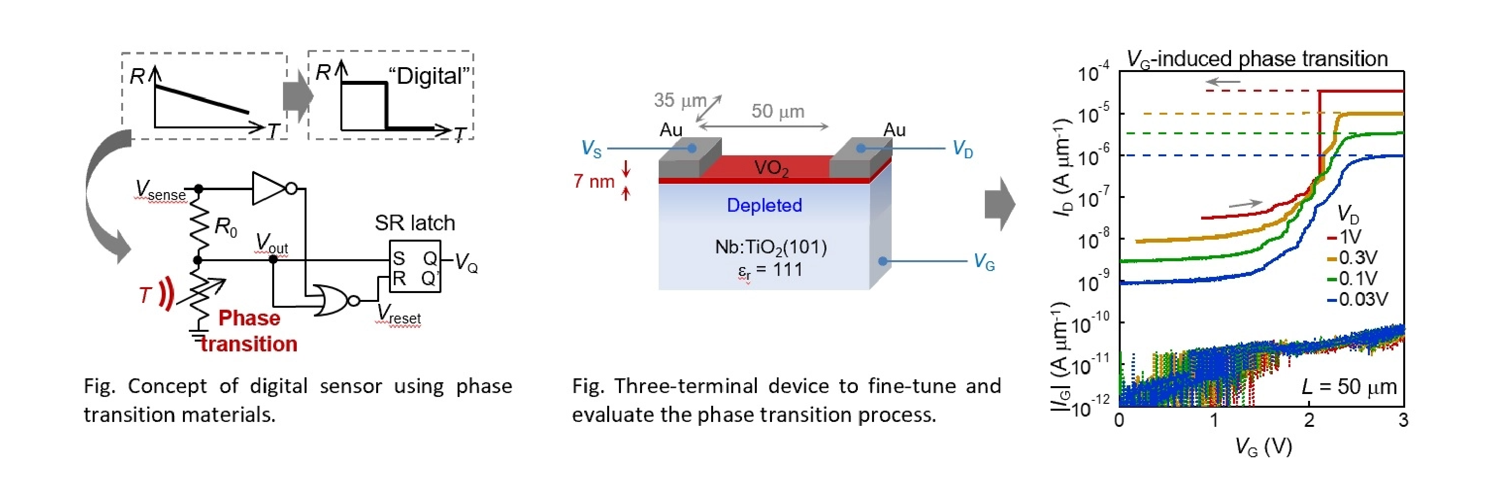
Sensors mediate between the real world and information space. Most conventional sensors extract information by “measuring” slight changes in the properties of the sensor material using electronic circuits such as AD converters. This method is good for accuracy and versatility, but it is redundant and wasteful for use in countless IoT devices. In fact, many of the sensor organs of biological neural circuits are thoroughly wasteless, as the sensors themselves have high non-linearity and extracts meaningful information. In this research, we are focusing on the phase transition of materials, which is a typical nonlinear phenomenon, and developing neuromorphic digital sensors that can be directly embedded in digital circuits, using the property that the property values change significantly across the transition. Since the material itself performs the “measurement”, it enables ultra-low power consumption and high-speed sensing, and therefore, we expect this to be a new framework for sensors that are not constrained by electronic circuits.
(ex) Ultra-low energy (several fJ) and high-speed (several ns) temperature sensor using VO2 metal-insulator transition
Takeaki Yajima Research Theme
y-2. Neuromorphic devices using electrons and protons(Working with M Corp.)
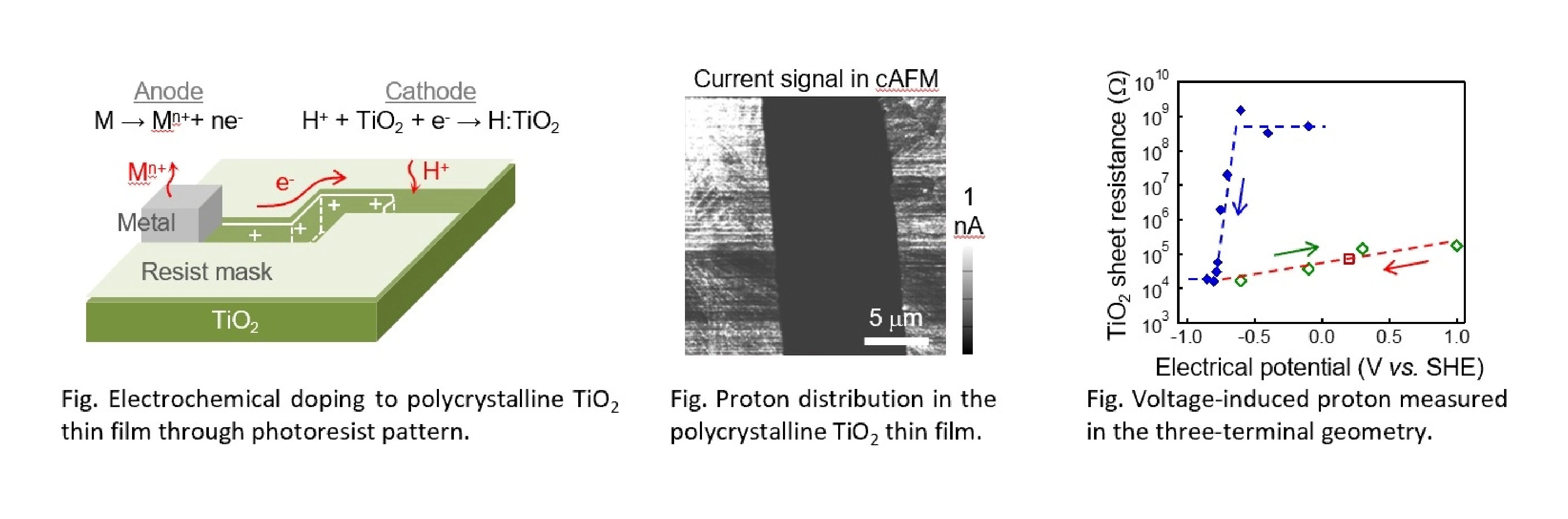
The performance of electronic circuits is constrained by the behavior of electrons. The trade-off between power consumption and speed is one of the examples of such constraints inherent to electronic circuits. On the other hand, ions play a major role in neural circuits, and the electrochemical role played by ions may allow us to break through the constraints or trade-offs that have been taken for granted in electronic circuits. In this research, we focus on the fact that the smallest ion, the proton, can move freely in solids, and by simultaneously controlling “electrons” and “protons” in solid-state devices, we can realize new functions that are fundamentally different from those of conventional electronics. We are trying to build a new field that combines phase transition physics and electrochemistry with the theory of electronics based on heterostructures.
(ex) Nanoscale proton distribution and its electrical control in oxide devices
Takeaki Yajima Research Theme
y-3. Ultra-low power information processing using spike signal
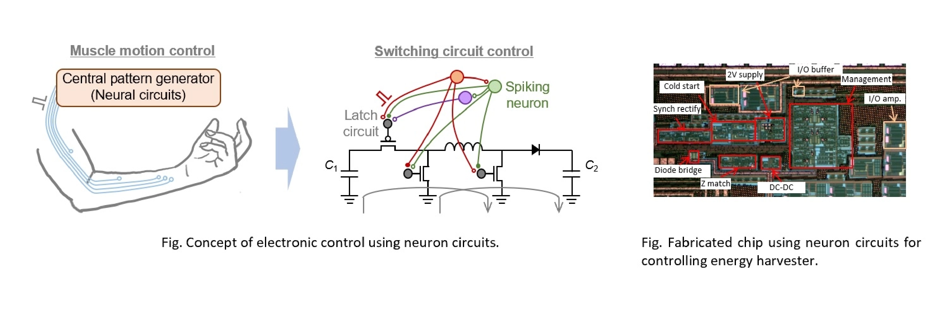
Countless IoT devices are attempting to interconnect the real world and information space. At this time, individual IoT devices are required to have unprecedentedly stringent low power consumption. Conventional devices process a large amount of information by ticking an internal time called “clock” independently from the real world, but they cannot meet the strict low power consumption requirements of the IoT. In this research, we focus on the fact that neural circuits in living organisms operate by coupling with the real world in real time via spike signals, and aim to realize real-time and lean electronic control based on spike signals.
(ex) Digital pattern generation using neuron circuitry and its application to power supply circuits for environmental power generation.
Takeaki Yajima Research Theme
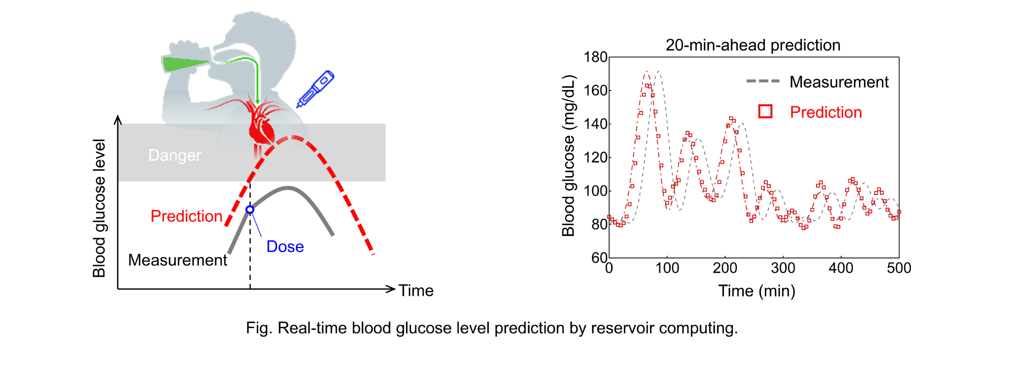
y-4. Ultra-low power learning circuits using reservoir computing and its application
In electronic circuits, information is represented by binary voltage signals (0/1), whereas in neural circuits, information takes entirely different forms, enabling flexible information processing not found in electronics. This research aims to develop an ultra-low-power learning circuit based on the reservoir computing algorithm, and to build hardware capable of flexibly performing anomaly detection and prediction by leveraging learning capabilities.
(ex) Prediction of biometric signals in wearable devices, anomaly detection in infrastructure monitoring
Satoshi Kawakami Research Theme
k-1. Noise-Driven Computer
情報処理に本当にエネルギーが必要なのでしょうか?この問に立ち向かう雑音駆動形の新計算原理を研究しています。本来,クロック信号によってスイッチングする超電導単一磁束量子回路を熱雑音で駆動する領域で活用し,可逆論理ゲートで演算を実現します。本研究では,人類の夢であるゼロ・エネルギーコンピューティングの実現に向け,計算原理・回路・アーキテクチャを刷新します。
Satoshi Kawakami Research Theme
k-2. Photonic Compute
シリコンフォトニクスやナノフォトニクスの技術が進展し,大量の光素子を集積することが可能になりつつあります。これにより,光子を情報担体とする計算機が実現可能となってきました。光速性と低電力性 (less than 1photon/OPs) を兼ね備える計算機を目指します。本研究では,現代の CMOSコンピュータとは一線を画す新しい光電融合型アクセラレータの実現します。
Satoshi Kawakami Research Theme
k-3. Ultra low power ASIC
あらゆる環境でのセンシングを想定するならばセンサノードの電力供給には環境発電を用い,尚且つ環境毎に適応的に駆動することが不可欠です。本研究では,効率的な環境発電を達成するために,環境発電用電源回路向け強化学習計算機を実現します。環境の微細な変化にセンサノード自らが適応し,最適な電力供給を元に稼働する完全自立型の汎用エナジーハーベストシステムを目指します。
Satoshi Kawakami Research Theme
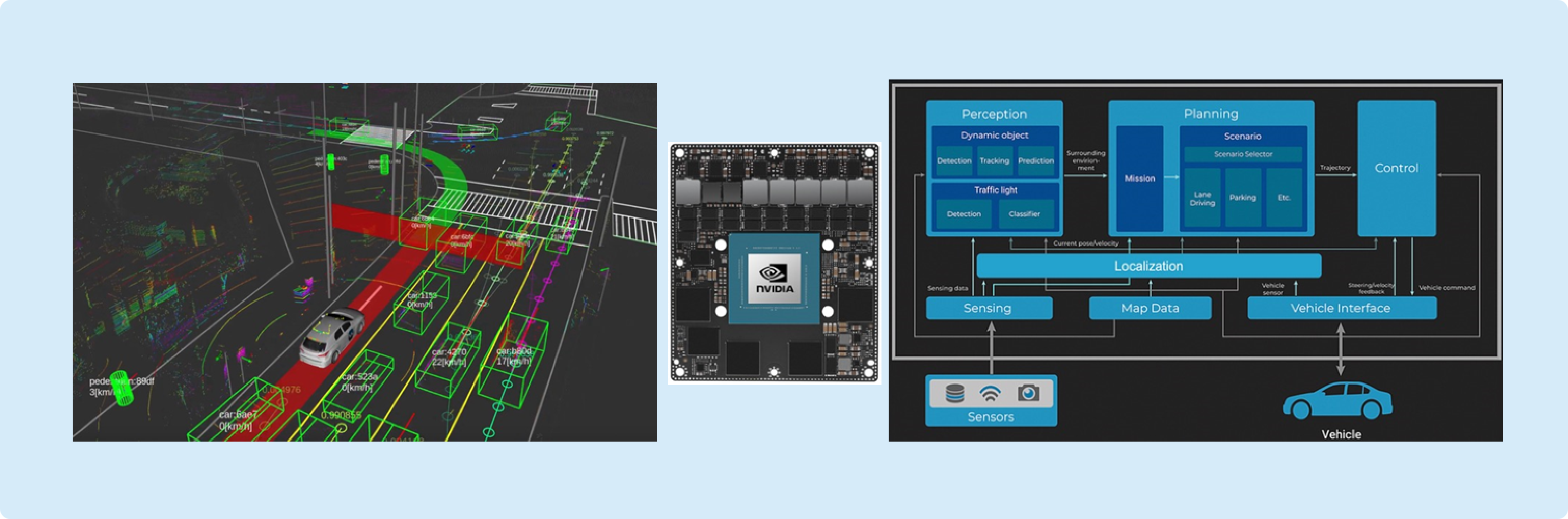
k-4. Self-driving Computer
自動運転の実現には,高性能・低電力な組み込みプロセッサーが不可欠です。特に,LiDARによる空間認識は,極めて短い時間に大量のデータを処理する必要があります。本研究では,車載のセンサー情報の収集・高速処理が可能な専用計算機の構築を実現します。企業連携による実計測データや仮想空間上でのシミュレーションを活用し,自動運転の実現に向けた社会実装を目指します。
Past Initiatives
Takeaki Yajima Kawakami Research Theme
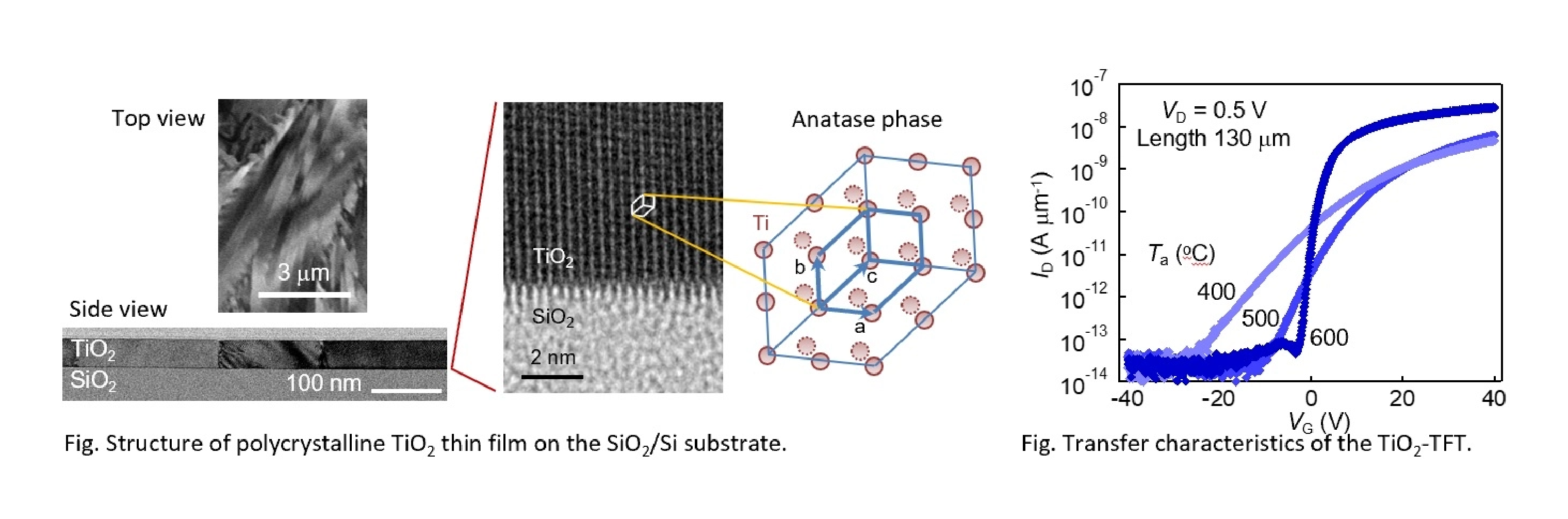
y-a. Wide-gap thin-film transistors
As typified by thin-film transistors for displays, thin-film transistors with high mobility can be mounted on a variety of substrates, creating significant added value. Various oxide semiconductors have been studied as channel materials for thin-film transistors, and although TiO2 is a well-known oxide semiconductor, there has been little research on thin-film transistors, and the reported field-effect mobility is less than 1 cm2/Vs, which is less than that of amorphous Si. On the other hand, the hole mobility of TiO2 polycrystalline thin films exceeds that of amorphous InGaZnO by more than 20 cm2/Vs, which raises the concern that the crystalline phase and the degree of freedom of crystal defects in TiO2 are not controlled during transistor fabrication. In this study, we have shown that the crystalline phase and crystalline defects can be independently controlled by the film-forming and heat-treatment processes of TiO2, and have demonstrated for the first time that field-effect mobility comparable to that of InGaZnO can be achieved in thin-film transistors using TiO2 (~10 cm2/Vs). This can be said to be the result of precisely controlling the internal degree of freedom of the material and extracting the true potential of TiO2.
Takeaki Yajima Kawakami Research Theme
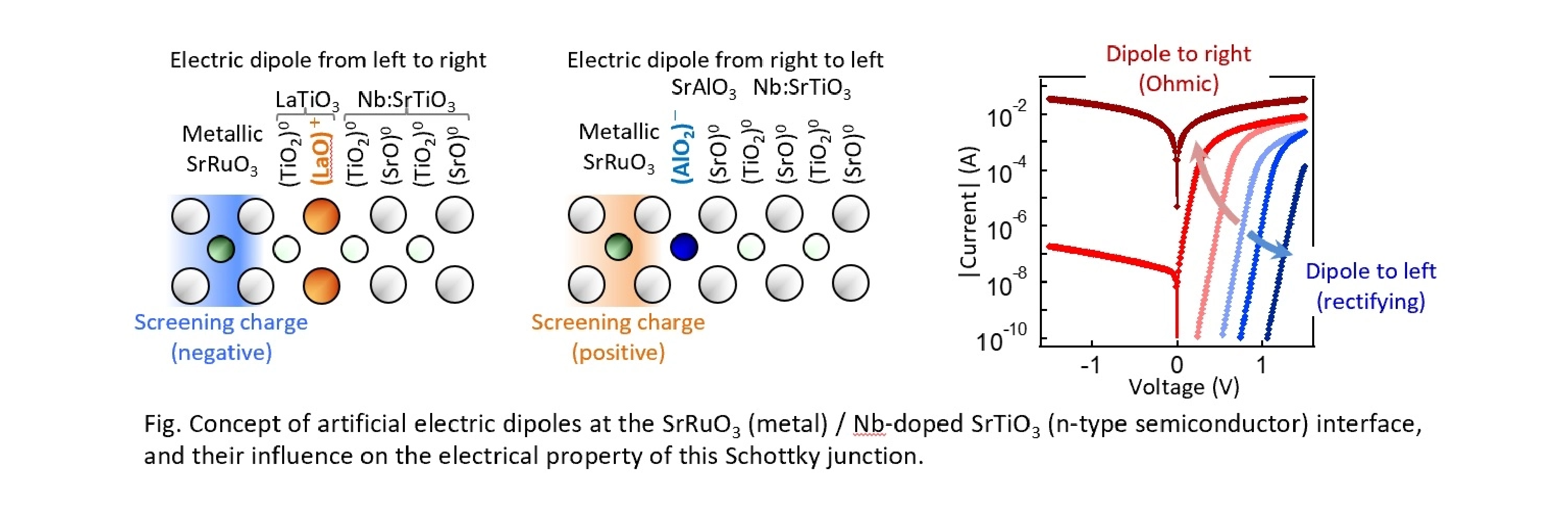
y-b. Dipole control of oxide epitaxial interfaces
The function of semiconductor devices such as transistors and solar cells is determined by the band alignment of electrons at the interface. Therefore, it would be ideal if the band alignment could be freely controlled, but in reality, the band alignment is uniquely fixed by the electronic energy of each material constituting the interface. In terms of electrostatics, the band alignment can be shifted by the size of the dipole moment by inserting positive and negative charge pairs into the interface. However, in semiconductor materials with strong covalent bonding, it is difficult to freely insert large interfacial dipoles. On the other hand, in oxide semiconductors with strong ionic bonding, it may be possible to design a large interfacial dipole by stacking positive and negative ionic charges at the atomic level. In this study, we have demonstrated that in a Schottky junction created by an epitaxial interface between SrRuO3 (metal) and SrTiO3 (N-type semiconductor), the band alignment can be significantly controlled in the range of about 2 eV by inserting ~Å-level positive and negative charge pairs at the interface. This dramatically changes the electrical properties of the junction interface, from diodes to ohmic junctions. In particular, we found that an atomically flat LaAlO3 layer with a thickness of less than 1 nm can change the band alignment as a dipole layer rather than as an insulator, which has recently been used in spin injection and photoelectrochemistry. Thus, we have shown that there is a large degree of freedom in the design of oxide interfaces that is unique to ionic bonding.
Takeaki Yajima Kawakami Research Theme
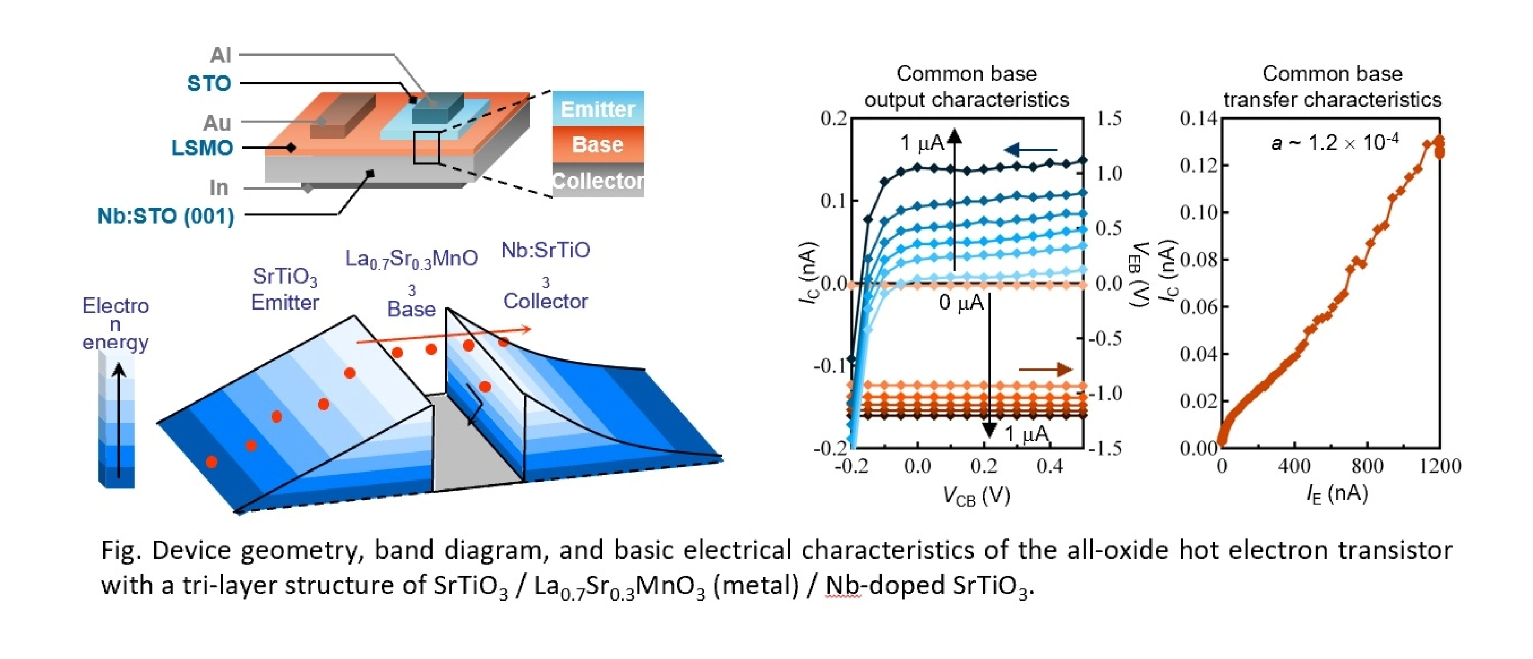
y-c. All-oxide hot electron transistors
In transition metal oxides with electrons in 3d orbitals, the electrons are in a more localized state than in semiconductors and metals composed of typical elements, and the interplay between the degrees of freedom of the electrons and the degrees of freedom of the lattice phonons causes a variety of phase transition phenomena. It is necessary to clarify how the electronic levels of materials change when multiple degrees of freedom are intertwined, and photoelectron spectroscopy and scanning tunneling spectroscopy have been used for this purpose. On the other hand, looking back at the history of semiconductors, it is possible to evaluate the mean free path of high-energy electrons (hot electrons) injected into a material through a tunneling or Schottky junction by fabricating a three-terminal device called a hot electron transistor. This should make it possible to measure the electron levels inside the material and their lifetimes very easily and with high sensitivity. In this study, we succeeded for the first time in demonstrating the operation of a hot electron transistor using transition metal oxide materials, and established a new research method for studying the properties of transition metal oxides.